Image

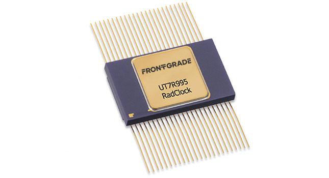
The UT7R995 is a low-voltage, low power, eight output, 6-to-200MHz clock driver.
The device features output phase programmability, which is necessary to optimize the timing of high-performance microprocessor and communication systems. The device also feature split output bank power supplies that enable banks 1 & 2, bank 3, and bank 4 to operate at a different power supply levels. The UT7R995 interfaces to a LVCMOS/LVTTL clock only.
Image left, text right (default)
- Features
- Eight Output Clock Driver
- +3.3V Core; +2.5V or +3.3V Clock Output Power Supply
- Independent Clock Output Bank Power supplies
- 6MHz to 200MHz Frequency
- <100ps Bank Pair Output-Output Skew
- <50px Cycle-Cycle Jitter
- 50% +/- 2% Maximum Output Duty Cycle @ 100MHz
- Eight LVTTL Outputs with Selectable Drive Strength
- Selectable Positive or Negative-Edge Synchronization
- Selectable Phase-Locked Loop (PLL) Frequency Range and Lock Indicator
- Phase Adjustments in 625 to 1300ps Steps Up to +/-7.8ns
- (1-6,8,10,12) x Multiply and (1/2,1/4) x Divide Ratios
- Compatible with Spread-Spectrum Reference clocks
- Power-down Mode
- Selectable Reference Input Divider
- Applications
- High-Performance Microprocessors
- Communication Systems
- Operational Environment
- Temperature Range: -55°C to +125°C
- Total Ionizing Dose: <100 krad (Si)
- SEL Immune: ≤109 MeV-cm2/mg
- Physical
- 48-Lead Ceramic Flatpack
- Power
- 1mW/MHz
- Flight Grade
- QML-Q, QML-V
- Export Control Classification Number (ECCN)
- 9A515.e.1
- SMD Number
- 5962-05214
ADDITIONAL SPECIFICATIONS
Datasheet
Application Notes
App_Note_UT7R995-Banks3Q+4QPhase_RevA
App-Note-UT7R995-RadClock-Jitter-BRM.pdf
App-Note-UT7R995-Current-Characterization-BRM.pdf
Product Brief
FG_UT7R995-EVB_RadClock_EVB_ProductBrief
IBIS Model
Do you need help with an existing product?
Our customer and technical support teams are happy to assist.
Image
Image
