
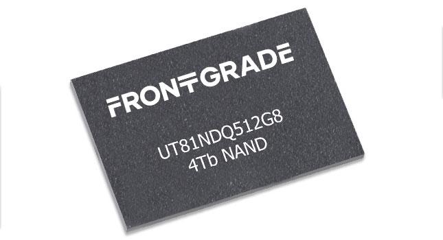
Frontgrade offers the highest density and highest performing NAND device in the space industry.
The UT81NDQ512G8T, 4Tb NAND flash based on the Triple-Level Cell (TLC) NAND technology delivers 32 times the density of the closest competing device available in a single industry standard JEDEC 132 BGA package.
The UT81NDQ512G8T is Open NAND Flash Interface (ONFI) 4.0 compliant and supports up to 667MT/s throughput (read/write) per pin. With access to unparalleled storage capacity, designers can significantly increase sensor and digital signal processing throughput in space instruments such as solid-state drives and recorders, reconfigurable computing systems and imaging and communications data buffering applications.
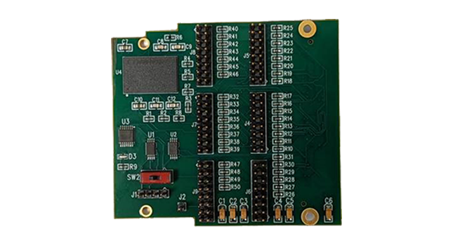
The UT81NDQ512G8T-KU060-EVB evaluation development board provides for a rapid prototyping platform interfacing to the Alpha Data KU060 kit utilizing the Xilinx KU060 Ultrascale FPGA. The EVB provides access to a single NAND through a VITA 57.1 compatible FMC and has options to startup the I/O at 1.8V or 1.2V.
- Features:
- 4Tb Density
- 3.3 V Core and 1.8 V, 1.2V I/O Supply Voltage
- Open NAND Flash Interface (ONFI) 4.0 Compliant
- Triple-Level Cell (TLC) Technology
- Organization
- Page Size: x8 18,592 Bytes
- Block Size: 2304 Pages
- Plane Size: 4 planes x 504 blocks
- Device Size: 16,128 Blocks
- Synchronous I/O Performance
- NV-DDR2 Support (533MT/s r/w throughput per pin)
- NV-DDR3 Support (667MT/s r/w throughput per pin)
- Asynchronous I/O Performance
- tRC/tWC: 20 ns (min)
- Array Performance
- Read Page: 74 uS (typical)
- Program Page: 1900 uS (typical)
- Erase Block: 15 ms (typical)
- Data Retention: JESD47G Compliant
- Endurance:
- 3 K Program/Erase Cycles (TLC mode)
- 40 K Program/Erase Cycles (SLC mode)
- Applications:
- Solid-State Drives
- Solid-State Recorders
- Reconfigurable Computing
- Imaging and Communications Data Buffering
- Space Computing
- Operational Environment:
- Temperature Range: -40°C to +85°C
- Total Ionizing Dose: <50 krad (Si)
- SEL Immune: ≤55 MeV-cm2/mg
- Physical:
- 132-Pin Plastic Ball Grid Array, JEDEC
- 12 mm x 18 mm, 1.0 mm pitch
- Power:
- <300mW (typical per active die)
- Flight Grade:
- PEM-INST-001 (NASA-EEE-INST-002) – Level 2
- Export Control Classification Number (ECCN):
- EAR99
ADDITIONAL SPECIFICATIONS
ECAD Models
Use the link(s) below to view the ECAD Model for this product.
Do you need help with an existing product?
Our customer and technical support teams are happy to assist.